CDM7-600LR TR13 PBFREE 数据手册
CDM7-600LR
SURFACE MOUNT SILICON
N-CHANNEL
LR POWER MOSFET
7.0 AMP, 600 VOLT
w w w. c e n t r a l s e m i . c o m
DESCRIPTION:
The CENTRAL SEMICONDUCTOR CDM7-600LR is a
600 Volt N-Channel MOSFET designed for high voltage,
fast switching applications such as Power Factor
Correction (PFC), lighting and power inverters. This
UltraMOSTM MOSFET combines high voltage capability
with ultra low rDS(ON), low threshold voltage, and low
gate charge for optimal efficiency.
MARKING: FULL PART NUMBER
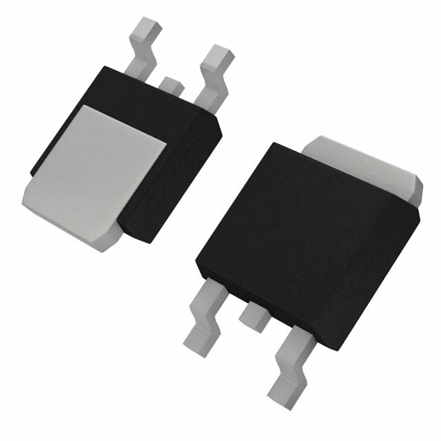
DPAK CASE
APPLICATIONS:
• Power Factor Correction
• Alternative energy inverters
• Solid State Lighting (SSL)
FEATURES:
• High voltage capability (VDS=600V)
• Low gate charge (Qgs=3.54nC TYP)
• Ultra low rDS(ON) (0.48Ω TYP)
MAXIMUM RATINGS: (TC=25°C unless otherwise noted)
SYMBOL
Drain-Source Voltage
VDS
Gate-Source Voltage
VGS
Continuous Drain Current (Steady State)
ID
Maximum Pulsed Drain Current, tp=10μs
IDM
Continuous Source Current (Body Diode)
IS
Maximum Pulsed Source Current (Body Diode)
ISM
Single Pulse Avalanche Energy (Note 1)
EAS
Power Dissipation
PD
Operating and Storage Junction Temperature
TJ, Tstg
Thermal Resistance
ΘJC
Thermal Resistance
ΘJA
600
30
7.0
28
7.0
28
255
60
-55 to +150
2.08
110
UNITS
V
V
A
A
A
A
mJ
W
°C
°C/W
°C/W
Note 1: L=79mH, IAS=2.4A, VDD=100V, RG=25Ω, Initial TJ=25°C
ELECTRICAL CHARACTERISTICS: (TC=25°C unless
SYMBOL
TEST CONDITIONS
IGSSF, IGSSR VGS=30V, VDS=0
IDSS
VDS=600V, VGS=0
BVDSS
VGS=0, ID=250μA
VGS(th)
VGS=VDS, ID=250μA
VSD
VGS=0, IS=7.0A
rDS(ON)
VGS=10V, ID=3.5A
Crss
VDS=100V, VGS=0, f=1.0MHz
Ciss
VDS=100V, VGS=0, f=1.0MHz
Coss
VDS=100V, VGS=0, f=1.0MHz
otherwise noted)
MIN
TYP
600
2.0
0.48
6.7
450
29
MAX
100
1.0
4.0
1.4
0.58
UNITS
nA
μA
V
V
V
Ω
pF
pF
pF
R4 (8-October 2020)
�CDM7-600LR
SURFACE MOUNT SILICON
N-CHANNEL
LR POWER MOSFET
7.0 AMP, 600 VOLT
ELECTRICAL
SYMBOL
Qg(tot)
Qgs
Qgd
td(on)
tr
td(off)
tf
trr
Qrr
CHARACTERISTICS - Continued: (TC=25°C unless otherwise noted)
TEST CONDITIONS
TYP
VDS=480V, VGS=10V, ID=7.0A (Note 2)
22.9
VDS=480V, VGS=10V, ID=7.0A (Note 2)
3.54
VDS=480V, VGS=10V, ID=7.0A (Note 2)
13.2
VDD=300V, VGS=10V, ID=7.0A, RG=24Ω (Note 2)
10.3
VDD=300V, VGS=10V, ID=7.0A, RG=24Ω (Note 2)
32.6
VDD=300V, VGS=10V, ID=7.0A, RG=24Ω (Note 2)
72.2
VDD=300V, VGS=10V, ID=7.0A, RG=24Ω (Note 2)
28.9
VGS=0, IS=7.0A, di/dt=100A/μs (Note 2)
430
VGS=0, IS=7.0A, di/dt=100A/μs (Note 2)
3.2
UNITS
nC
nC
nC
ns
ns
ns
ns
ns
μC
Note 2: Pulse Width < 300μs, Duty Cycle < 2%
DPAK CASE - MECHANICAL OUTLINE
SYMBOL
A
B
C
D
E
F
G
H
J
K
L
M
N
P
R
DIMENSIONS
INCHES
MILLIMETERS
MIN
MAX
MIN
MAX
0.083 0.108
2.10
2.75
0.016 0.032
0.40
0.81
0.035 0.063
0.89
1.60
0.203 0.228
5.15
5.79
0.020
0.51
0.016 0.024
0.40
0.60
0.051 0.071
1.30
1.80
0.248 0.268
6.30
6.81
0.197 0.217
5.00
5.50
0.209 0.245
5.30
6.22
0.025 0.040
0.64
1.02
0.090 0.115
2.30
2.91
0.012 0.045
0.30
1.14
0.180
4.60
0.090
2.30
DPAK (REV: R1)
PIN CONFIGURATION
LEAD CODE:
1) Gate
2) Drain
3) Source
4) Drain
Pin 2 is common to the tab (4)
MARKING: FULL PART NUMBER
R4 (8-October 2020)
w w w. c e n t r a l s e m i . c o m
�CDM7-600LR
SURFACE MOUNT SILICON
N-CHANNEL
LR POWER MOSFET
7.0 AMP, 600 VOLT
TYPICAL ELECTRICAL CHARACTERISTICS
R3 (21-May 2020)
w w w. c e n t r a l s e m i . c o m
�OUTSTANDING SUPPORT AND SUPERIOR SERVICES
PRODUCT SUPPORT
Central’s operations team provides the highest level of support to insure product is delivered on-time.
• Supply management (Customer portals)
• Custom bar coding for shipments
• Inventory bonding
• Custom product packing
• Consolidated shipping options
DESIGNER SUPPORT/SERVICES
Central’s applications engineering team is ready to discuss your design challenges. Just ask.
• Free quick ship samples (2nd day air)
• Special wafer diffusions
• Online technical data and parametric search
• PbSn plating options
• SPICE models
• Package details
• Custom electrical curves
• Application notes
• Environmental regulation compliance
• Application and design sample kits
• Customer specific screening
• Custom product and package development
• Up-screening capabilities
REQUESTING PRODUCT PLATING
1. If requesting Tin/Lead plated devices, add the suffix “ TIN/LEAD” to the part number when
ordering (example: 2N2222A TIN/LEAD).
2. If requesting Lead (Pb) Free plated devices, add the suffix “ PBFREE” to the part number
when ordering (example: 2N2222A PBFREE).
CONTACT US
Corporate Headquarters & Customer Support Team
Central Semiconductor Corp.
145 Adams Avenue
Hauppauge, NY 11788 USA
Main Tel: (631) 435-1110
Main Fax: (631) 435-1824
Support Team Fax: (631) 435-3388
www.centralsemi.com
Worldwide Field Representatives:
www.centralsemi.com/wwreps
Worldwide Distributors:
www.centralsemi.com/wwdistributors
For the latest version of Central Semiconductor’s LIMITATIONS AND DAMAGES DISCLAIMER,
which is part of Central’s Standard Terms and Conditions of sale, visit: www.centralsemi.com/terms
w w w. c e n t r a l s e m i . c o m
(001)
�